Tokyo Institute of Technology, “SubRISC +” CPU architecture for IoT. Energy efficiency 3.8 times – per hour
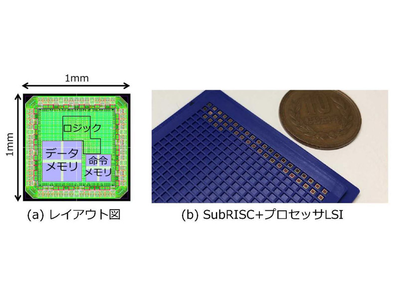

SubRISC + chip layout and LSI prototype
Yuko Hara, Assistant Professor of Information and Communications at the College of Engineering, Tokyo Institute of Technology, announced at the age of 19 that she has designed the “SubRISC +” energy-efficient compact / CPU architecture.
We have limited the functionality to process the required computations of small terminals in practical time, and have achieved both miniaturization and energy saving. Even if LSI was manufactured using a 65nm CMOS process, it achieved a small size of 1x1mm and achieved a low power consumption of 77μm. It is said that it can handle practical applications such as anomaly detection and real time data search.
Edge computing is indispensable for spreading the Internet of Things, but current CPUs are difficult to deploy from a power consumption point of view. This is because there are more than enough instructions to meet the varied applications. For example, for embedded 32-bit systems, even very small systems handle about 50 types of instructions (Cortex). -M0 has 60 types, RISC-V Micro-riscy has 47 types). Therefore, the circuit area and power consumption increase.
Compared with existing processors
SubRISC + is designed for use in the real-time processing of lightweight algorithms that detect anomalies and search for data from the data, and send only limited data such as warnings. By limiting the number of instructions to four, we aim to reduce size and power consumption. On the one hand, it is a complete Turing and can handle general purpose software other than these purposes.
SubRISC + architecture
As an example of the program, we implemented a lightweight algorithm that could detect epileptic seizures in real time from acceleration data and verify their effectiveness. The power was 131.1 μW.
Lightweight algorithm
Compared to the same processing that Arm’s commercial Cortex-M0 CPU does, it is 1.4 times faster, 2.7 times more energy efficient, and 3.8 times more energy efficient.
When the architecture was actually implemented with a 65nm process, the overall size of the LSI was as small as 1 x 1mm, and power consumption when driving at 5MHz (a frequency that could secure real-time processing sufficiently to detect healthcare anomalies). It was only 77 μW. This is a test account that can run continuously for about 100 days using the LR44 button battery, and the energy efficiency is said to be extremely high.
In the future, in addition to considering distributing prototype samples and displaying at exhibitions, the company plans to expand SubRISC + to prototypes and implement practical use chips that allow a wider range of applications.

Andrew Prescott is a contributor to Prudent Press Agency, covering a wide range of topics including news, politics, business, technology, sports, entertainment, and lifestyle. He focuses on delivering clear, balanced reporting and practical information that helps readers stay informed about current events and emerging developments. His work highlights stories that matter to everyday audiences, with an emphasis on accuracy, relevance, and accessible journalism.