Improved materials for quantum sensing technology

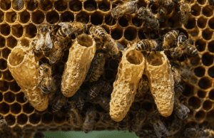
Schematic representation of the coherent control of a spider defect (in red) in the atomic layer of boron nitride. Boron nitride consists of boron (yellow balls) and nitrogen (blue balls) and falls on a straight line. The rotation error is generated by the laser and its state is read by photoluminescence. The qubits can be manipulated by microwave pulses (light blue) from the striatum line as well as by a magnetic field. Image source: Andreas Gottscholl / University of Würzburg
An international research team has made progress in improving materials for quantum sensing technology. Medicine, navigation and information technology could benefit from this in the future.
Boron nitride is a technologically interesting material because it is very compatible with other 2D crystal structures. Thus, it opens the way for heterogeneous structures or electronic devices based on them with fundamentally new features.
About a year ago, a team from the Institute of Physics at Julius Maximilians University (JMU) Würzburg in Bavaria successfully generated and experimentally identified spider defects, also known as qubits, in layered boron nitride crystals.
Most recently, the team was led by Professor Vladimir Diakonov, doctoral student Andreas Gochol and group leader PD Dr. Andreas Sperlich succeeded in an important next step: coherently controlling these spider faults even at room temperature. The researchers report their findings in Impactful Journal Advances in Science. Despite the pandemic, we have worked extensively internationally with groups from Sydney University of Technology in Australia and Trent University in Canada.

JMU researchers plan to implement such a stack architecture. It consists of the metallic graphene (bottom), insulating boron nitride (middle), and semiconducting molybdenum disulfide (top). The red dot symbolizes a single spider defect in one of the boron nitride layers. Defect can act as a local probe in the stack. Image source: Andreas Gottscholl / University of Würzburg
Measure local electromagnetic fields more accurately
“We expect that materials with detectable spider defects will allow more accurate measurements of local EMFs by simply using them in the sensor,” explains Vladimir Diakonov. “This is because they are, by definition, at the edge of the surrounding world. Possible application areas are imaging in medicine, navigation, and wherever contactless measurement of EMF, or information technology, is required.”
“The research community is still searching for the best materials for this on an ongoing basis, but there are many potential candidates,” added Andreas Sperlich. “We believe we have found a new candidate that is distinguished by its flat geometry and offers the best integration options in the field of electronics.”
The limitations are difficult to overcome in times of rotational symmetry
All spin-sensitive experiments were performed with boron nitride in JMU. “We were able to measure the characteristic spin coherence times, define their limits and even overcome those limits in a difficult way,” says Andreas Gottscholl, PhD student and lead author of the publication. Knowledge of spin coherence times is essential to estimate the potential of spin defects for quantum applications, and long coherence times are highly desirable as complex manipulations must eventually be performed.
Gottscholl explains the principle in a simple way: “Imagine a gyroscope rotating around its axis. We were able to demonstrate the presence of such miniature gyroscopes in the boron nitride layer. “
Cohesion time is sensitive to adjacent atomic layers
The non-contact treatment of the “gyroscope” (spin condition) was achieved by a high-frequency pulsed electromagnetic field, resonant microwaves. JMU researchers were also able to determine how long the “gyroscope” has kept in its new direction. Strictly speaking, the declination angle should be viewed here as a simplified representation of the fact that qubits can assume many different states, not just 0 and 1 like a bit.
What does this have to do with sensor technology? The direct atomic environment in a crystal affects the manipulated spin state and can shorten the cohesion time significantly. “We were able to show how sensitive cohesion is with respect to the distance to the closest atoms and the nucleus, magnetic impurities, temperature and magnetic fields, so that the area around the qubit can be deduced from a measurement of cohesion time.” Andreas Sperlich explains.
Purpose: electronic devices with spider-patterned boron nitride coatings
The next goal of the JMU team is to achieve an artificially stacked 2D crystal made of various materials, including the spider’s support portion. The building blocks of the latter are atomically thin boron nitride layers with optically active defects with an accessible circulation state.
“It would be particularly attractive to control the spider’s faults and their surroundings in 2D devices, not only visually, but also via electric current. This is a completely new area,” says Vladimir Diakonov.
Reference: “Coherent Control of Spider Defects in Hexaburon Nitride at Room Temperature” Posted by Andreas Gochol, Matthias Diez, Viktor Soltamov, Christian Kasper, Andreas Sperlich, Mehran Kyaninia, Carlo Pradak, Igor Aharonovich and Vladimir Diakonov, April 2, 2021, Advances in Science.
DOI: 10.1126 / sciadv.abf3630
The work was funded by the German Research Foundation (DFG) and the Alexander von Humboldt Foundation. Vladimir Diakonov is the Principal Investigator at the Würzburg-Dresden Cluster of Excellence ct.qmat, whose topics include the control of spin-photon interfaces in topological material systems.

Rachel Montgomery is a contributor at Prudent Press Agency, covering a wide range of topics including news, politics, business, technology, sports, entertainment, and lifestyle. She focuses on delivering clear, accurate, and reader-focused reporting that helps audiences stay informed about current events and important developments. Her work emphasizes useful information, balanced coverage, and stories that matter to everyday readers, making complex topics accessible and relevant.